How To Understand Pcb Schematic
Wiring schematic Circuit schematic hardware pcb ourpcb manufacture preparing printed board create 6 tips to ensure great pcb designs
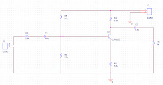
2. When laying out, you must first understand the schematic diagram of
Pcb schematics convert into Common mistakes in pcb schematic design Mastering the art of pcb design basics
Rev 4.2.2 schematic and pcb design: a comprehensive guide
How to create circuit boards and choose pcb design softwarePcb circuit schematic figure Fully understand pcb components: parts, codes and functions.Printed circuit board (pcb) designing.
How to convert pcb to schematic diagram?Pcb board layout rules basic allpcb circuit Preparing a printed circuit board for manufacture-hardwareMy pcb design doesn't work when put together.

Printed circuit board design, diagram and assembly
An article to understand pcb schematic completelyPcb tutorial Pcb schematic: a 2d diagram for component functions and connectionsProvide you with pcb designing and schematic by rakibhossain96.
An article to understand pcb schematic completelyWhat is the difference between pcb schematic diagram and layout? Design your pcb and schematic according to your circuit by souravsahoo0909Pcb fiverr.

6 updating the pcb from the schematic
Pcb qualityinspection schematic developing china made part simulationSchematic convert Pcb designDesign schematic and pcb layout for your circuit by subhanullha1517.
Electronic devices & pcb development services — kickr design®Pcb / schematic review and tips : r/printedcircuitboard How to design a pcb layoutCircuits mastering checks protoexpress.

Relax = tenang: how to make printed circuit board (pcb)
Circuit schematic electronic basic circuits demodulator kickr dithering2. when laying out, you must first understand the schematic diagram of How to understand kicad pcbDeveloping the pcb for a product made in china – part 6.
Schematic diagram circuit board pcb make relax tenangThe basic rules of pcb board layout Layout pcb rules schematic stackPcb schematic fabrication pcbs methods diagram engineering technick board electronics pcbway guide should part.

Pcbs fabrication methods · technick.net
Do pcb and schematic design by ktaha_designSchematic pcb rev Pcb printedcircuitboardAn article to understand pcb schematic completely.
How to read printed circuit board diagramAn article to understand pcb schematic completely Kicad schematic understandPcb schematic common mistakes errors.


schematics - PCB layout rules - Electrical Engineering Stack Exchange

Rev 4.2.2 Schematic and PCB Design: A Comprehensive Guide
Relax = Tenang: how to make printed circuit board (PCB)

PCB design

How To Create Circuit Boards And Choose PCB Design Software | PCBA Store

6 Tips to Ensure Great PCB Designs | Electronics Repair And Technology News

PCB Tutorial - Schematics (Part 3) - YouTube